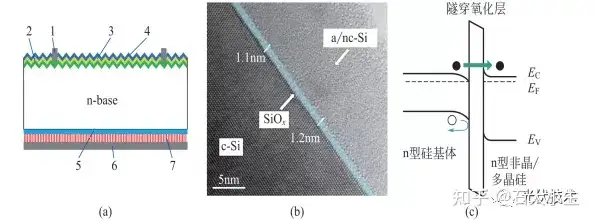
Tunneling oxide Tunnel Oxide Passivated Contact solar cell (TOPcon) is a new type of passivated contact solar cell first proposed by the Fraunhofer Institute for Solar Energy Research in Germany at the 28th European PVSEC Photovoltaic Conference in 2013. First, a 1-2nm tunnel oxide layer is prepared on the back of the cell, and then a layer of doped polysilicon is deposited. The two together form a Passivated contact structure , providing good interface passivation for the back side of the silicon wafer.
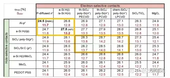
The ultimate efficiency of the battery composed of different electron/hole selective contact materials is 28.7%, and the current maximum conversion efficiency of the full-area battery is 25.4%;
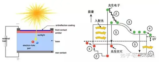
The energy of incident photons with long wavelengths is smaller than the bandgap of the material, resulting in Incident light Directly through the cell—low energy photon loss;
The incident light energy is much higher than the bandgap width of the material, resulting in High Energy Electrons - Hole pairs are lost by thermal relaxation due to collision with the crystal lattice - High Energy Photons loss;
Electron and hole crossover PN Junction Compound loss;
Recombination losses of electrons and holes in the electrode contact area;
Electrons and holes are lost by recombination within the substrate/at the interface;
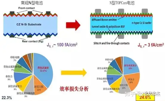
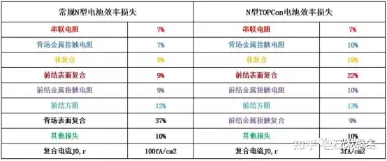
The key factor restricting the further improvement of the efficiency of traditional crystalline silicon (c-Si) solar cells is Metal Electrode The loss caused by carrier recombination at the interface between Jo and silicon causes the Jo load current to be high.
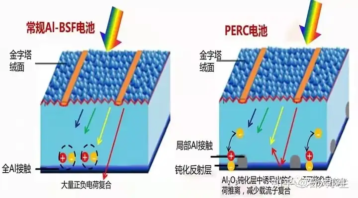
Conventional AL-BSF (Aluminium Back Surface Field) Aluminum back field Since the metal electrode on the back of the solar cell is in direct contact with Si, the back is fully metal-compounded, and the carrier recombination is serious, resulting in a high J0 and a Voc that is difficult to exceed 685mv. The current maximum efficiency is 20.3%, and it has basically been eliminated by the market;
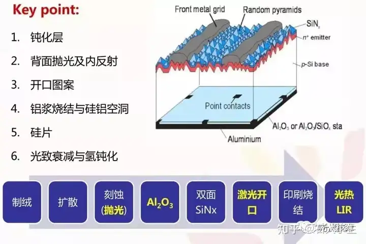
After adopting PERC back passivation contact technology, since AL2O3/SiNx are both dielectric insulating films, local holes need to be opened in the dielectric film to achieve electrical contact, which causes the carriers to be collected by the metal electrode through two-dimensional transport, resulting in lateral resistance transport loss. FF decreases with the increase of metal contact spacing. At the same time, the local contact between metal and Si still has a high recombination in this area, that is, Jo, metal is relatively high, and Voc cannot exceed 700mv. The current highest efficiency is 24.06%. According to ISFH calculations, the theoretical limit efficiency of PERC cells is 24.5%;
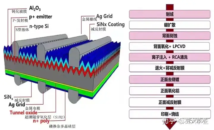
The silicon oxide between the Poly-Si and Si substrate interface of the TOPCon passivated contact cell plays a very critical role in passivation. Chemical passivation The interface state density between the Si substrate and Poly-Si is reduced, and the majority carrier concentration is much higher than the minority carrier concentration. While reducing the probability of electron-hole recombination, it also increases the resistivity to form selective contact for the majority carriers.
In the selective contact area, the majority carrier transmission leads to resistance loss, while a small amount of minority carriers migrate to the metal contact area, resulting in recombination loss. Contact resistance pc, the latter corresponds to the interface composite J0, currently J0 is as low as 2fA/cm2, pc is as low as 3mΩ/cm2 n+Poly Passivated Contact , Voc is as high as 733mv, the battery Voc exceeds 700mv, and the current maximum efficiency is 25.4%. According to ISFH calculations, the theoretical limit efficiency of TOPCon batteries is 28.7%;
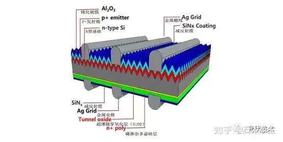
5.1 Due to its special Band structure The ultra-thin oxide layer allows majority carriers to tunnel but blocks minority carriers from penetrating. Depositing a layer of metal as an electrode on it can realize a passivation contact structure without opening holes.
5.2 No need for laser drilling, using N-type silicon wafer No light-induced degradation, compatible with medium and high temperature sintering;
5.3 The main passivation improvement is the back passivation, which uses a 1-2nm high-quality SiOx layer combined with doping Amorphous Silicon High temperature crystallization annealing is performed to achieve full area passivation contact, using high quality Ultra-thin silicon oxide and doped polysilicon layer to achieve efficient passivation and selective carrier collection on the entire back side;

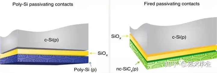
Compared with the existing PERC, the core structure of TOPCon is an ultra-thin silicon dioxide layer. Quantum tunneling effect , which can allow electrons to pass smoothly and prevent the recombination of holes.
7.1 The full-area passivation surface eliminates the silicon/metal contact interface, which is beneficial to improving the open circuit voltage Voc, while the full-area carrier collection reduces the lifetime sensitivity, which is beneficial to improving the fill factor FF;
7.2 Blocking the passage of minority carriers while allowing majority carriers to pass easily without obstacles, thus reducing recombination;
7.3 Structure Passivation layer It can inhibit the carrier recombination on the surface of silicon wafer and improve the Minority life span The carrier selective collection passivation contact structure can be applied to the entire surface of the battery without opening holes to form local passivation contacts, which not only simplifies the manufacturing process but also allows carriers to be transported in only one dimension without the need for additional Horizontal transmission, thus achieving a higher fill factor;
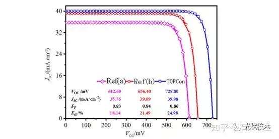
The cells Ref (a) (b) in the figure above are cells without silicon oxide passivation. Compared with cell a, cell b has an additional heavily doped n+-poly-Si layer on the back surface, while TOPCon has a double-sided passivation function of silicon oxide, making Voc, Jsc, FF and Eff the highest, reaching 729.8mV, 39.98mA/cm2, 0.86 and 24.98% respectively.
Compared with the Ref(b) cell with back field function, the Jsc of the TOPCon cell only increased by 0.89mA/cm2, an increase of 2.3%, while the Voc increased by 73.4mV, an increase of 11.2%. This shows that the passivation of the front and back surfaces of crystalline silicon by silicon oxide can greatly reduce the recombination of carriers on the front and back surfaces of the cell, increasing the battery's Open circuit voltage , thereby improving the efficiency of the battery.
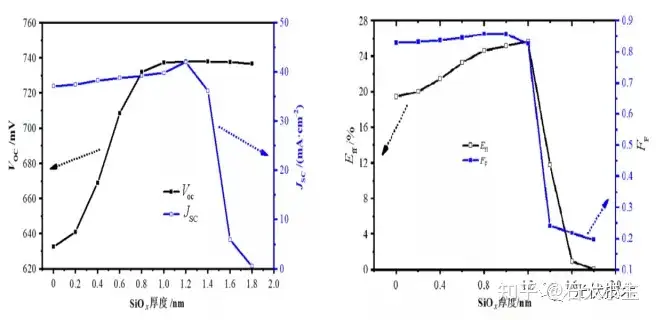
The influence of silicon oxide thickness on the performance of TOPCon cells. With the increase of thickness, Voc increases rapidly and then remains basically unchanged. When the thickness of silicon oxide is 1.2nm, Voc reaches a maximum value of 738.1mV. The other three battery parameters Jsc, FF and Eff have basically the same trend with the change of silicon oxide thickness. They first increase slowly and then decrease rapidly with the increase of thickness. When the thickness of silicon oxide is 1.2nm, Jsc and Eff reach the maximum values of 42.02mA/cm2 and 26.8% respectively, indicating that there is an optimal value (1.2nm) for the thickness of silicon oxide in TOPCon cells. When the thickness of silicon oxide is greater than 1.2nm, the efficiency of the cell begins to drop sharply.
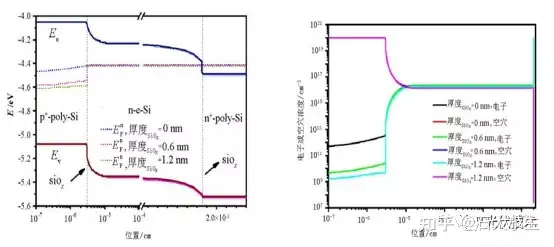
When SiOx is not present, its electron Fermi level (EnF) There is a slight Discontinuous , this discontinuity has little impact on the majority carriers (electrons). However, when a thin layer of SiOx is inserted, a very obvious discontinuity of the electron quasi-Fermi level appears at the p+-poly-Si/nc-Si interface. Under open circuit conditions, the net recombination rate of carriers is equal to the net generation rate. The insertion of oxide prevents the majority carriers in nc-Si from flowing to the front surface to recombine with holes, which to a certain extent reduces the recombination of nc-Si with p+-poly-Si and the front electrode. In addition, the electron concentration in nc-Si is greater than that of holes, and there is a lower electron concentration in the high recombination area. It is precisely because of the discontinuity of the electron quasi-Fermi level that the discontinuity between SiOx and nc-Si occurs. Recombination Rate of reduction.
The concentrations of electrons and holes in nc-Si are basically close, but the electron concentration is still greater than the hole concentration, indicating that although electrons are not easy to tunnel through SiO x at the front interface, they are easy to tunnel through at the back interface. At the same time, holes do not form a discontinuity of the quasi-Fermi level. Holes on the front surface are easy to tunnel through, while the back surface forms a certain barrier to holes. This shows that the passivation effect is reflected in the transport of carriers, that is, the role of the passivation interface state.
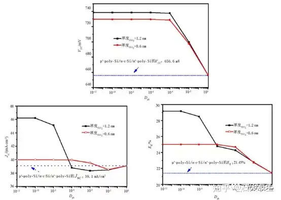
The mesopore density (Dph) of silicon oxide characterizes the defect density in silicon oxide. The tunneling of carriers in silicon oxide with distributed mesopore density is essentially the transport of carriers in two-dimensional space. However, when the thickness of silicon oxide is several nm, this two-dimensional carrier transport can be approximated as one-dimensional transport. When Dph is lower than 10-6, the highest Voc can reach about 740mV, as shown in Figure 5. This shows that low mesopore density has almost no effect on Voc. When Dph is between 10-6 and 10-4, the effect on Voc can also be ignored.
The influence of Dph on the Jsc of TOPCon cells. When Dph increases from 10-12 to 10-6, when the silicon oxide thickness is 0.6nm, Jsc remains at 40.0mA/cm2 with almost no change. However, when the silicon oxide thickness is 1.2nm, Jsc decreases significantly from 46.2mA/cm2 to 38.8mA/cm2, which is lower than the Jsc of the device without silicon oxide passivation.
This shows that the greater the thickness of silicon oxide, the greater the influence of mesopore density on short-circuit current, the greater the mesopore density of silicon oxide, the worse the passivation effect of the device, and the Leakage Current When the mesopore density is greater than 10-2, the effect of the mesopore density on the short-circuit current is no longer related to the silicon oxide thickness.
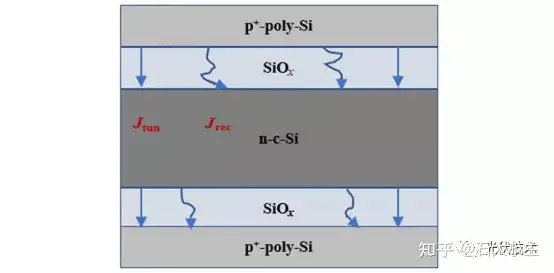
Pinholes cause direct contact between polysilicon and crystalline silicon to form a high recombination current (Jrec). In addition, electrons tunnel directly from polysilicon through silicon oxide to form a tunneling current (Jtun).
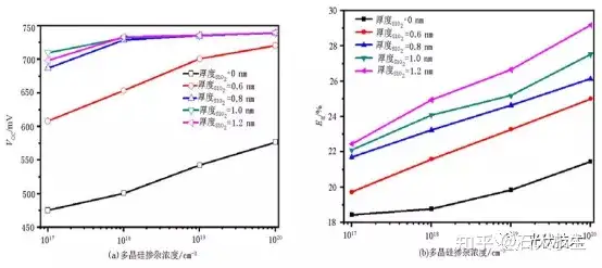
For traditional pn junction c-Si solar cells, the higher the doping concentration of the emitter layer, Depletion Region The larger the built-in electric field, the smaller the Photogenerated carriers The number of minority carriers injected from the other side of the pn junction is only about Thermal balance The number of minority carriers in the material is determined by the doping concentration. Reducing the minority carrier concentration can reduce recombination, while increasing the doping concentration can minimize the minority carrier concentration. However, high doping will lead to a decrease in the carrier diffusion length, thereby increasing carrier recombination.
Therefore, in traditional pn junction c-Si solar cells, there is an optimal emitter layer doping concentration. Polysilicon layer The thickness of the polysilicon layer is only 30nm, so the phenomenon of reduced diffusion length without high doping concentration does not occur. In addition, high doping in the p+ or n+ polysilicon layer increases the tunneling probability of electrons or holes in silicon oxide. Therefore, the higher the doping concentration of the polysilicon layer, the higher the open circuit voltage and efficiency of the TOPCon solar cell.
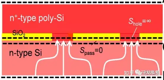
When the silicon oxide thickness is less than 2nm, the carriers are mainly transported by tunneling;
When the silicon oxide thickness is greater than 2nm, carriers are mainly transmitted through pinholes in the silicon oxide layer. Although the high pinhole density is beneficial to transmission, it is not conducive to passivation and carrier transmission will be limited.