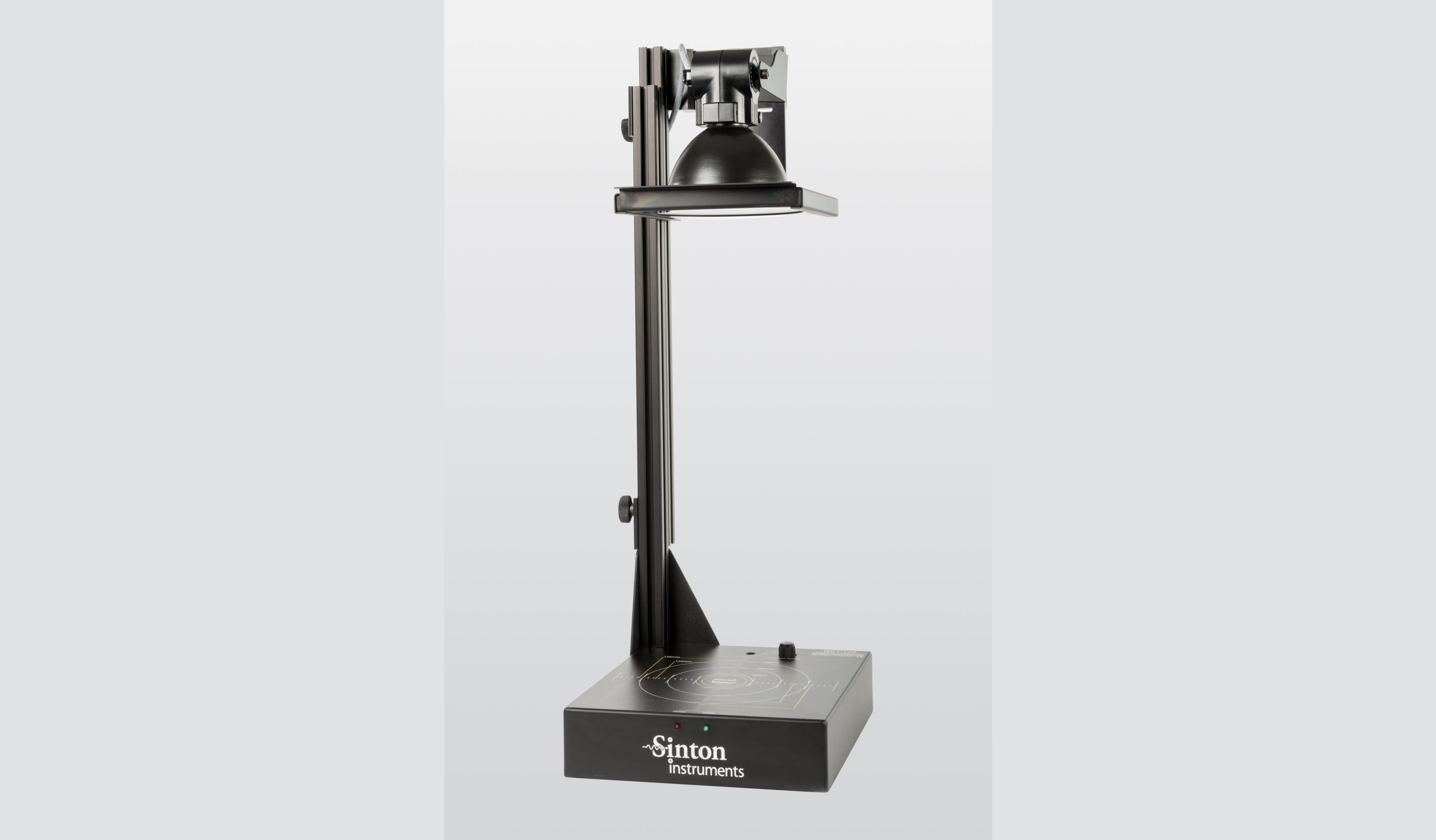

The silicon wafer test instrument provides the best available technology for calibrated analysis of carrier recombination lifetime, fully compliant with SEMI standard PV-13.
The WCT-120 is a desktop silicon wafer lifetime measurement system suitable for device research and industrial process control at an affordable price. The WCT-120MX is suitable for testing larger size silicon wafers of 230mm.