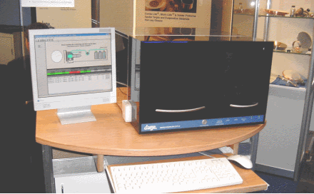
• Electrochemical ECV doping concentration detection Electrochemical CV distribution instrument (CV tester) Electrochemical CV profile analyzer Electrochemical CV carrier concentration junction depth tester
  • Electrochemical ECV doping concentration detection Electrochemical CV distribution instrument (CV tester) Electrochemical CV profile analyzer Electrochemical CV carrier concentration junction depth tester
  • Electrochemical ECV doping concentration detection Electrochemical CV distribution instrument (CV tester) Electrochemical CV profile analyzer Electrochemical CV carrier concentration junction depth tester
  • Electrochemical ECV doping concentration detection Electrochemical CV distribution instrument (CV tester) Electrochemical CV profile analyzer Electrochemical CV carrier concentration junction depth tester

Electrochemical ECV doping concentration detection Electrochemical CV distribution instrument (CV tester) Electrochemical CV profile analyzer Electrochemical CV carrier concentration junction depth tester

No.CVP21

The equipment is suitable for evaluating and controlling epitaxial processes in semiconductor production and can be used on a variety of different materials, such as: Silicon, Germanium, III-V including III-Nitrides.


CVP21 The clean room and modular system design structure enable this system to measure the doping concentration distribution in semiconductor materials (structures, layers) efficiently and accurately. Select appropriate electrolyte to contact and corrode the material, so as to obtain the doping concentration distribution of the material . Capacitance voltage scanning and corrosion process are fully automatically controlled by software

联系资深销售技术支持
联系资深销售技术支持
GET A QUOTE
  • Electrochemical ECV doping concentration detection Electrochemical CV distribution instrument (CV tester) Electrochemical CV profile analyzer Electrochemical CV carrier concentration junction depth tester
  • Electrochemical ECV doping concentration detection Electrochemical CV distribution instrument (CV tester) Electrochemical CV profile analyzer Electrochemical CV carrier concentration junction depth tester
  • Description

  • Specifications

  • Contact Us

Electrochemical ECV doping concentration detection Electrochemical CV distribution instrument (CV tester) Electrochemical CV profile analyzer Electrochemical CV carrier concentration junction depth tester

Fully automatic electrochemistry CV Distributor CVP21 The choice of photovoltaic solar energy field! The choice of many scientific research and semiconductor users!
Shanghai Shunmiao Optoelectronics Official China Fully automatic electrochemistry CV Distributor Photovoltaic solar energy agent! Serving many well-known photovoltaic companies!

The equipment is suitable for evaluating and controlling epitaxial processes in semiconductor production and can be used on a variety of different materials, such as: Silicon, Germanium, III-V including III-Nitrides.


CVP21 The clean room and modular system design structure enable this system to measure the doping concentration distribution in semiconductor materials (structures, layers) efficiently and accurately. Select appropriate electrolyte to contact and corrode the material, so as to obtain the doping concentration distribution of the material . Capacitance voltage scanning and corrosion process are fully automatically controlled by software
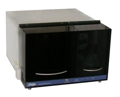
CVP21
System Features
Robust and reliable modular system structure .The optics, electronics and chemistry parts are relatively independent.
Precise measurement circuit module
Powerful control software, system operation, easy to use
Complete after-sales service system

Electrochemical ECV doping concentration detection Electrochemical CV distribution instrument (CV tester) Electrochemical CV profile analyzer Electrochemical CV carrier concentration junction depth tester Crystalline silicon is especially recommended Solar Battery research unit use

ECV/Junction Depth Tester/Diffusion Concentration Sorter
ECV (model:
CVP21 ) is widely used in the solar photovoltaic industry, with a market share of more than 95%. It is one of the necessary tools for the research and development of battery technology in the photovoltaic industry, and is used by almost all well-known photovoltaic companies.

WEP's ECV equipment:
CVP21 (See picture)
1. ECV is also known as diffusion concentration tester, junction depth tester, etc., that is, the electrochemical CV method measures the carrier concentration distribution after diffusion (see figure);
2. Compared with other methods such as SRP, SIMS, etc., ECV has the advantages of easy measurement and low price;

  1. WEP's ECV has a unique technology that can be applied to test velvet samples of battery cells, which is one of the reasons why it is widely used;
  1. CVP21 The measurable depth range is nm---10um;
    5. No calibration is required when the measured carrier concentration range is within 10e12cm-3 < N < 10e21cm-3;
    6. When measuring diffusion samples, the samples are kept "Dry in" and "Dry out" and no special treatment is required;
    7. The chemical reagents used can be purchased locally, the price is low and the amount used is small. One purchase can be used for several years;
    8. The data measured by CVP21 can provide three kinds of information to R&D or process personnel: surface concentration, concentration change curve, and junction depth (see figure);
    9. Surface concentration is helpful for selecting and using suitable slurry, such as matching issues such as adhesion and contact resistance;
    10. The concentration distribution curve provides a basis for mastering and improving the diffusion process;
    11. The information of junction depth is necessary for the overall grasp of battery technology, and it is also one of the items that need to be sampled during the diffusion process;
    12. Reference: Several diffusion concentration distribution curves tested (see figure);
    13. Extensive customer base: Q-CELL, NREL, ISFH, SHELL, ECN, RWE, HMI, SISE, Suntech, Trina Solar, JA Solar, Yingli, Jiaoda Taiyang, BYD, Harun, JinkoSolar, Jiyang, CSG, GreenPower...
Electrochemical ECV doping concentration detection Electrochemical CV distribution instrument (CV tester) Electrochemical CV profile analyzer Electrochemical CV carrier concentration junction depth tester

Quality Service

  1. Free sample testing is available and test reports are provided.
  2. Warranty period: 2 years, lifetime maintenance.
  3. We promise users lifetime free sample testing once a month.

Electrochemical CV distribution instrument (CV tester)
Product Manager: Mike Zhai
Contact number: 021- 34635258/59/61/62
hand Phone: 13681980050
mail box:
mike@rayscience.com

CVP21 Download detailed information

Electrochemical ECV Doping concentration detection Electrochemistry CV distribution instrument (CV tester) Electrochemistry CV Profile Analyzer Electrochemistry CV carrier concentration

http://www.rayscience.com/cv/27594.pdf
http://www.rayscience.com/cv/ECVBSF.pdf
http://www.rayscience.com/cv/ECVPKHALLSIMSSRP.pdf
http://www.rayscience.com/cv/flyer-cvp21.pdf
http://www.rayscience.com/cv/Heterojunctions.pdf
http://www.rayscience.com/cv/ISFH.pdf
http://www.rayscience.com/cv/ISFHECV.pdf
http://www.rayscience.com/cv/KonstanzECV-Profiles.pdf
http://www.rayscience.com/cv/Letter_of_Excellence_Distributor_for_Rayscience.pdf
http://www.rayscience.com/cv/semiconductortoday.pdf
http://www.rayscience.com/cv/wepsellscvp21.pdf

Technical parameters:

We have over 30 years of experience in electrochemical distribution testing products and the most advanced circuit systems in the world.

Fully automatic, especially suitable for new materials such as gallium nitride, silicon carbide, etc.

Effective inspection: epitaxial materials, diffusion, ion implantation
Applicable materials: CVP21 has a wide range of applications and can be used for most semiconductor materials.
Group IV compound semiconductors such as silicon (Si), germanium (Ge), silicon carbide (SiC), etc.;
III-V compound semiconductors such as gallium arsenide (GaAs), indium phosphide (InP), gallium phosphide (GaP), etc.;
Ternary III-V compound semiconductors such as aluminum gallium arsenide (AlGaAs), gallium indium phosphide (GaInP), aluminum indium arsenide (AlInAs), etc.;
Quaternary III-V compound semiconductors such as aluminum gallium indium phosphide (AlGaInP), etc.
Nitrides such as gallium nitride (GaN), aluminum gallium nitride (AlGaN), indium gallium nitride (InGaN), aluminum indium nitride (AlInN), etc.;
II-VI compound semiconductors such as zinc oxide (ZnO), cadmium telluride (CdTe), mercury cadmium telluride (HgCdTe), etc.;
Other uncommon semiconductor materials (please contact us for sample measurement).

Carrier concentration measurement range:
*Maximum 1021/cm³; Minimum 1011/cm³
Depth resolution: unlimited; minimum down to 1 nm (or less)
Modular system structure: Topological structure, real-time monitoring of corrosion process, suitable for tiny samples and large-sized wafers, fully automated system.


Key Features:

CVP21 electrochemical ECV is the perfect solution for semiconductor carrier concentration distribution:
1. CVP21 has a wide range of applications and can be used for most semiconductor materials.
* Group IV compound semiconductors such as silicon (Si), germanium (Ge), silicon carbide (SiC), etc.;
* III-V compound semiconductors such as gallium arsenide (GaAs), indium phosphide (InP), gallium phosphide (GaP), etc.;
* Ternary III-V compound semiconductors such as aluminum gallium arsenide (AlGaAs), gallium indium phosphide (GaInP), aluminum indium arsenide (AlInAs), etc.;
* Quaternary III-V compound semiconductors such as aluminum gallium indium phosphide (AlGaInP), etc.
* Nitrides such as gallium nitride (GaN), aluminum gallium nitride (AlGaN), indium gallium nitride (InGaN), aluminum indium nitride (AlInN), etc.;
* II-VI compound semiconductors such as zinc oxide (ZnO), cadmium telluride (CdTe), mercury cadmium telluride (HgCdTe), etc.;
* Other uncommon semiconductor materials (please contact us for sample measurement).
2. CVP21 can be used for samples of different forms: multi-layer thin film materials, no restrictions on substrates (substrates can be conductive or insulating), standard sample sizes range from 4*2mm to 8-inch wafers (please consult us in advance for smaller size samples).
3. CVP21 has a good resolution range.
* Carrier concentration resolution ranges from < 1012 cm-3 to > 1021 cm-3
* Depth resolution ranges from 1nm to 100um (depending on sample type and sample quality)
4. CVP21 is a complete electrochemical ECV measurement system.
* High system reliability (the electronic, mechanical, optical and liquid transmission parts of the instrument are specially designed)
* Calibration-free system (fully self-calibrating electronic system, cable capacitance does not require user recalibration)
* Ease of use (full user management software optimized for ease of use in lab or production environments)
* Camera lens control (the process is controlled online by a color camera lens; the lens data can be retrieved after each measurement.)
* Experimental menu (predefined measurement menus, which can be easily modified or improved by privileged users)
* Dry-In/Dry-Out: Auto-Load/Unload/Reload (Electrochemical sample cell automatic loading/unloading/reloading, priority user easy to modify, sample dry-in/dry-out processing.)
Shanghai Sales + Technical Support + After-sales Service Center
Rayscience Optoelectronic Innovation Co., Ltd

address: 4th Floor, Building 122, Lane 2338, No. 1 Duhui Road, Minhang District, Shanghai
Telephone:
021-34635258 021-34635259
fax:
021-34635260
E-mail:
saleschina@rayscience.com

Download